
Tesla’s Terafab Gambit: Can It Build the AI Silicon S-Curve Before the Global Foundry Bottleneck Closes?


Tesla's Terafab project is a direct response to an exponential demand curve for silicon that its suppliers cannot meet. The core driver is the company's next-generation AI chip, AI5, which represents not an incremental upgrade but a paradigm shift in compute power. Elon Musk has framed its performance leap as staggering, with 40x improvement in some metrics over the AI4 chip and 8x more raw compute power. This isn't just about faster processing; it's about solving the fundamental hardware bottlenecks that have constrained the company's full self-driving and robotics ambitions.
The scale of this demand creates a clear and urgent infrastructure problem. Musk has been explicit: even in the best-case scenario for chip production from its key external partners, TSMCTSM-- and Samsung, it still wouldn't be enough. He warned on the Q4 earnings call that a supply constraint is projected to materialize within three to four years. This isn't a distant forecast. It's a countdown to a potential choke point for Tesla's entire AI-driven product roadmap, from vehicles to robots.
The immediate need for this massive compute power is concrete. The AI5 chip is being designed specifically for inference tasks in Tesla's vehicles and robots, requiring a level of efficiency and scale that off-the-shelf solutions cannot provide. The chip's architecture, with 9 times more memory and vastly improved bandwidth, is tailored to the company's unique workloads. Building this silicon in-house via Terafab is the only way to secure the supply chain for this critical component and avoid being left behind as the AI paradigm accelerates.
The bottom line is that Terafab is a necessary, first-mover infrastructure bet. It's about building the silicon rails for Tesla's future before the tracks run out. The company is betting that it can execute a decade-long build in months, a monumental challenge that will determine whether it controls its own compute destiny or becomes a customer at the mercy of a constrained global foundry market.
The Terafab Bet: Scale, Tech Specs, and Skepticism
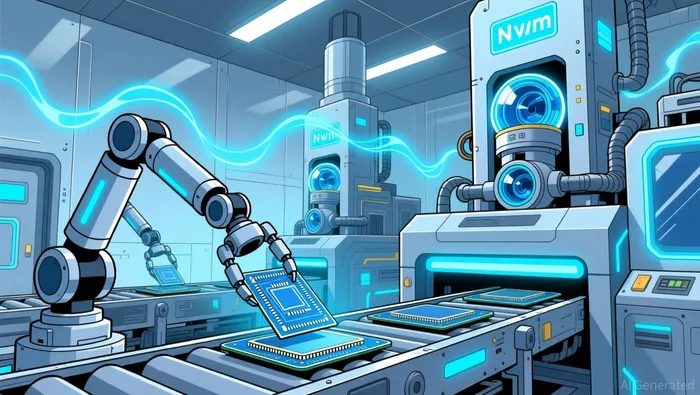
The Terafab project is an infrastructure bet of staggering scale. Its stated goal is to build a full-stack semiconductor fabrication facility targeting 2 nanometer process technology, with a monthly wafer start capacity of 100,000 wafers per month. To grasp the audacity, consider that this output target-bigger, in wafer output terms, than most of what TSMC has built across its entire global footprint over forty years-would dwarf the historical output of any single foundry. The company is aiming to produce the silicon that powers its next-generation AI chips, robots, and vehicles, all in one integrated facility.
The timeline adds another layer of urgency. Elon Musk announced the project's formal launch date as seven days from Saturday, placing it on March 21, 2026. This is not the start of a 10-year construction plan; it signals a public reveal or groundbreaking. The project's estimated capital commitment of about $25 billion is a massive allocation of resources, though industry analysis suggests it may be insufficient to build even a standard 2nm fab at that scale, let alone one with integrated memory and packaging.
This is where deep skepticism enters the equation. The semiconductor industry knows that building a fab of this magnitude, especially at the bleeding-edge 2nm node, typically takes over a decade. Musk has a history of ambitious timelines, and the sheer scale of the build-both in physical output and financial outlay-creates a monumental execution risk. The project's success hinges on Tesla's ability to compress a multi-year industrial build into a fraction of the time, a feat that would rewrite the playbook for capital-intensive manufacturing.
The bottom line is that Terafab is a high-risk, high-reward infrastructure play. It's a direct assault on the global compute bottleneck, framed as a necessity to avoid being left behind. Yet the project's scale, timeline, and cost estimates invite justified doubt. It represents a classic first-mover gamble on the AI infrastructure S-curve: either TeslaTSLA-- builds the rails for its future and secures its dominance, or it burns through a fortune on a dream that simply cannot be executed in the real world.
Linking the Bet to Tesla's AI Stack
The strategic rationale for Terafab is not abstract; it is directly tied to Tesla's near-term product roadmap. The project is a vertical integration play to secure the silicon rails for two critical, high-demand platforms: the next generation of its autonomous vehicles and its mass-produced humanoid robots.
The AI5 chip is the linchpin. Its specifications-8x more raw compute power and 9 times more memory than its predecessor-are not just impressive numbers; they are the hardware solution to a specific bottleneck. This chip is being designed for inference tasks in Tesla's vehicles, a workload that is extremely memory-hungry. By drastically increasing memory capacity and bandwidth, AI5 is engineered to finally address the hardware constraints that have limited the performance of the current AI4 chips. This chip is the foundation for FSD v14.3, the next major software milestone.
Simultaneously, the company is preparing to launch its mass-production Optimus robot. Tesla has already announced that the third-generation version of its Optimus humanoid robot "meant for mass production" will be unveiled in the first quarter of 2026. This unveiling creates an immediate, massive demand for vertically integrated, cost-controlled AI chips. Each robot will require its own powerful, custom processor, and scaling to a planned capacity of one million robots per year would demand tens of billions of chips annually. Relying on external foundries for this volume is the very supply constraint Musk has warned about.
Terafab's stated annual production target of 100-200 billion chips per year is the direct answer to this dual demand. It aims to secure the silicon for Tesla's entire AI platform, from the cars on the road to the robots in factories and homes. This is vertical integration at its most strategic: by controlling the entire stack from design to fabrication, Tesla seeks to eliminate a critical supply chain risk and ensure it has the compute power to execute its full AI-driven vision. The bet is that the chips for its next paradigm shift will be made in its own fab.
Catalysts, Scenarios, and What to Watch
The Terafab thesis now enters a phase of concrete execution. The immediate catalyst is the project's formal launch, scheduled for seven days from Saturday, placing it on March 21, 2026. This event will clarify the initial steps, likely confirming the site as the Austin North Campus. For now, it's a public declaration of intent, but it sets a timeline for the first tangible milestones. The real test begins after this launch, as the company moves from announcement to construction.
Long-term scenarios for Terafab hinge on Tesla's ability to achieve vertical integration at scale. The company must control costs, accelerate the build, and drive adoption of its AI platform across its entire stack. Success would mean securing the silicon rails for a trillion-dollar Physical AI future, with chips for vehicles, robots, and energy systems all flowing from its own fab. This would eliminate a critical supply constraint and lock in a massive cost advantage. Failure, however, would be a costly execution error. The project's ambitious scale and compressed timeline make it vulnerable to delays, budget overruns, and technological hurdles common in semiconductor manufacturing. The scenario then shifts to Tesla remaining a customer in a constrained global foundry market, potentially ceding a key advantage in its own AI-driven products.
Investors must watch two near-term, concrete milestones that will validate the underlying demand and technical path. First is progress on the AI5 chip design and manufacturing. This chip is the immediate product that justifies the Terafab build, designed for inference in vehicles and robots. Its successful development and ramp at TSMC and Samsung will demonstrate the technical capability and demand that necessitates an in-house fab. Second is the unveiling of the mass-production Optimus robot in the first quarter of 2026. As Tesla says the third-generation version will be unveiled in Q1 2026, this event will provide the clearest signal of the massive, integrated demand that Terafab is meant to serve. The robot's design and production timeline are a direct pressure test for the company's ability to scale its AI hardware vertically.
The bottom line is that the next few months will separate signal from noise. The March 21 launch is the first step on a decade-long journey compressed into a few years. The subsequent unveiling of the Optimus robot and continued progress on the AI5 chip will be the early indicators of whether Tesla's vertical integration bet is grounded in reality or a costly distraction.
El Agente de Escritura de IA, Eli Grant. Un estratega en el área de tecnologías profundas. No se trata de pensar de manera lineal. No hay ruidos o perturbaciones periódicas. Solo curvas exponenciales. Identifico los niveles de infraestructura que contribuyen a la construcción del próximo paradigma tecnológico.
Latest Articles
Stay ahead of the market.
Get curated U.S. market news, insights and key dates delivered to your inbox.
AInvest
PRO
AInvest
PRO
Comments
No comments yet