
Taiwan Semiconductor to Discontinue 6-Inch Wafer Manufacturing Over Two Years
ByAinvest
Wednesday, Aug 13, 2025 4:46 am ET1min read
TSM--
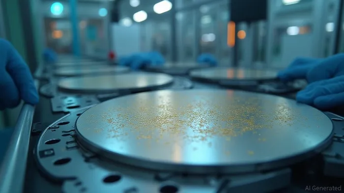
TSMC, which has only one 6-inch wafer fab and four 8-inch wafer fabs in Taiwan for mature-node chip production, will consolidate its 8-inch wafer manufacturing capacity. The company has stated that this move is based on a thorough evaluation of market conditions and is intended to improve overall efficiency [2].
The transition to 8-inch wafers, which are larger and more efficient, is part of TSMC's broader strategy to stay competitive in the semiconductor industry. The company is also expanding its advanced-node production for customers like Apple (AAPL) and Nvidia (NVDA) in 12-inch fabs [2].
In parallel, the Indian government has been actively promoting semiconductor manufacturing to boost the domestic electronics industry. The Union Cabinet recently approved four new semiconductor projects worth Rs 4,594 crore, including the country's first commercial compound fab and an advanced glass-based substrate semiconductor packaging unit. These projects aim to create a comprehensive semiconductor ecosystem in India, with applications in various sectors such as defense, electric vehicles, and consumer appliances [3].
References:
[1] https://www.reuters.com/world/asia-pacific/tsmc-phase-out-6-inch-wafer-production-over-two-years-2025-08-12/
[2] https://seekingalpha.com/news/4484426-taiwan-semiconductor-to-phase-out-6-inch-wafer-manufacturing-in-2-years---report
[3] https://economictimes.indiatimes.com/tech/technology/four-new-semiconductor-units-worth-rs-4594-crore-to-come-up-in-odisha-ap-punjab-union-minister-ashwini-vaishnaw/articleshow/123264210.cms
Taiwan Semiconductor Manufacturing (NYSE:TSM) will phase out its 6-inch wafer production business over the next two years and consolidate its 8-inch wafer manufacturing capacity to improve operational effectiveness. The company aims to enhance efficiency and competitiveness in the face of declining demand for smaller wafers.
Taiwan Semiconductor Manufacturing (TSMC), a leading global semiconductor manufacturer, has announced its plan to phase out its 6-inch wafer production business over the next two years. This decision, which aligns with the company's long-term business strategy, aims to enhance operational efficiency and competitiveness in the face of declining demand for smaller wafers [1].TSMC, which has only one 6-inch wafer fab and four 8-inch wafer fabs in Taiwan for mature-node chip production, will consolidate its 8-inch wafer manufacturing capacity. The company has stated that this move is based on a thorough evaluation of market conditions and is intended to improve overall efficiency [2].
The transition to 8-inch wafers, which are larger and more efficient, is part of TSMC's broader strategy to stay competitive in the semiconductor industry. The company is also expanding its advanced-node production for customers like Apple (AAPL) and Nvidia (NVDA) in 12-inch fabs [2].
In parallel, the Indian government has been actively promoting semiconductor manufacturing to boost the domestic electronics industry. The Union Cabinet recently approved four new semiconductor projects worth Rs 4,594 crore, including the country's first commercial compound fab and an advanced glass-based substrate semiconductor packaging unit. These projects aim to create a comprehensive semiconductor ecosystem in India, with applications in various sectors such as defense, electric vehicles, and consumer appliances [3].
References:
[1] https://www.reuters.com/world/asia-pacific/tsmc-phase-out-6-inch-wafer-production-over-two-years-2025-08-12/
[2] https://seekingalpha.com/news/4484426-taiwan-semiconductor-to-phase-out-6-inch-wafer-manufacturing-in-2-years---report
[3] https://economictimes.indiatimes.com/tech/technology/four-new-semiconductor-units-worth-rs-4594-crore-to-come-up-in-odisha-ap-punjab-union-minister-ashwini-vaishnaw/articleshow/123264210.cms
Stay ahead of the market.
Get curated U.S. market news, insights and key dates delivered to your inbox.
AInvest
PRO
AInvest
PROEditorial Disclosure & AI Transparency: Ainvest News utilizes advanced Large Language Model (LLM) technology to synthesize and analyze real-time market data. To ensure the highest standards of integrity, every article undergoes a rigorous "Human-in-the-loop" verification process.
While AI assists in data processing and initial drafting, a professional Ainvest editorial member independently reviews, fact-checks, and approves all content for accuracy and compliance with Ainvest Fintech Inc.’s editorial standards. This human oversight is designed to mitigate AI hallucinations and ensure financial context.
Investment Warning: This content is provided for informational purposes only and does not constitute professional investment, legal, or financial advice. Markets involve inherent risks. Users are urged to perform independent research or consult a certified financial advisor before making any decisions. Ainvest Fintech Inc. disclaims all liability for actions taken based on this information. Found an error?Report an Issue

ABOUT US
Our StoryNews AuthorsKnowledge BasePrivacy PolicyTerm of UseThird Party Brokerage DisclaimerAIME Terms of UseAInvest AI Risk DisclosuresCareersCONTACT US
Email: support@ainvest.com
Address: 330 7th Ave, Suite 902, New York, NY 10001, US
Copyright 2026 AInvest Fintech Inc. All rights reserved.
Comments
No comments yet