
Infinitesima launches three-year development project with ASML to enhance Metron3D 300mm wafer metrology system for cutting-edge applications.
ByAinvest
Tuesday, Jul 22, 2025 2:14 pm ET1min read
ASML--
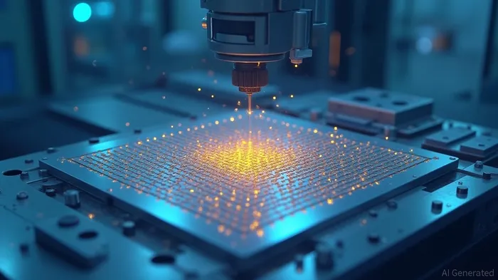
ABINGDON, United Kingdom, July 2, 2025 — Infinitesima Limited, a UK-based leader in advanced metrology solutions for the semiconductor industry, has announced a three-year development project aimed at enhancing the capabilities of its Metron3D 300mm in-line wafer metrology system [1]. The project, which includes partnerships with ASML and imec, seeks to optimize metrology solutions for cutting-edge applications such as hybrid bonding, high-NA EUV lithography, and 3D logic device structures.
The Metron3D system, which features Infinitesima’s Rapid Probe Microscope (RPM™) technology, will be used to address the industry's urgent need for detailed 3D metrology information throughout the full structure of features at high throughput and in high-volume manufacturing environments [1]. The system will be sited at imec, a world-leading research and innovation hub in nanoelectronics and digital technologies, to advance next-generation device development [1].
Infinitesima’s partnership with imec began in 2021, initially focusing on enabling tip-induced nanoscale tomographic sensing using its patented RPM™ for research and failure analysis applications [1]. This new collaboration marks the expansion of the Infinitesima-imec partnership into high-speed, in-line production metrology, supporting the semiconductor industry’s advancing inspection and metrology demands for sub-nanometer features and increasingly complex 3D structures [1].
The project aims to deliver true 3D process control, which is critical for enabling the production of future semiconductor devices. Peter Jenkins, CEO of Infinitesima, stated, “We are delighted to extend our existing collaboration with imec to support the critical metrology challenges of some of the most critical process steps for next-generation semiconductor processes” [1].
Infinitesima's leading position in in-line semiconductor metrology is set to be reinforced through this expanded partnership, supporting the industry's evolution toward smaller and increasingly complex device architectures [1].
References
[1] https://finance.yahoo.com/news/infinitesima-begins-project-further-develop-060000684.html
[2] https://www.globenewswire.com/news-release/2025/07/22/3119157/0/en/Infinitesima-Begins-Project-to-Further-Develop-the-Capabilities-of-the-Metron3D-300-mm-In-line-Wafer-Metrology-System.html
Infinitesima has begun a three-year project to develop the capabilities of its Metron3D 300mm in-line wafer metrology system. The system will be used to optimize metrology solutions for applications such as hybrid bonding, high-NA EUV lithography, and 3D logic device structures. Infinitesima will work with partners including ASML and imec to deliver true 3D process control, critical for enabling the production of future semiconductor devices. The project aims to address the industry's need for detailed 3D metrology information throughout the full structure of features at high throughput and in high-volume manufacturing environments.
Title: Infinitesima Launches Three-Year Project to Enhance Metron3D 300mm In-line Wafer Metrology SystemABINGDON, United Kingdom, July 2, 2025 — Infinitesima Limited, a UK-based leader in advanced metrology solutions for the semiconductor industry, has announced a three-year development project aimed at enhancing the capabilities of its Metron3D 300mm in-line wafer metrology system [1]. The project, which includes partnerships with ASML and imec, seeks to optimize metrology solutions for cutting-edge applications such as hybrid bonding, high-NA EUV lithography, and 3D logic device structures.
The Metron3D system, which features Infinitesima’s Rapid Probe Microscope (RPM™) technology, will be used to address the industry's urgent need for detailed 3D metrology information throughout the full structure of features at high throughput and in high-volume manufacturing environments [1]. The system will be sited at imec, a world-leading research and innovation hub in nanoelectronics and digital technologies, to advance next-generation device development [1].
Infinitesima’s partnership with imec began in 2021, initially focusing on enabling tip-induced nanoscale tomographic sensing using its patented RPM™ for research and failure analysis applications [1]. This new collaboration marks the expansion of the Infinitesima-imec partnership into high-speed, in-line production metrology, supporting the semiconductor industry’s advancing inspection and metrology demands for sub-nanometer features and increasingly complex 3D structures [1].
The project aims to deliver true 3D process control, which is critical for enabling the production of future semiconductor devices. Peter Jenkins, CEO of Infinitesima, stated, “We are delighted to extend our existing collaboration with imec to support the critical metrology challenges of some of the most critical process steps for next-generation semiconductor processes” [1].
Infinitesima's leading position in in-line semiconductor metrology is set to be reinforced through this expanded partnership, supporting the industry's evolution toward smaller and increasingly complex device architectures [1].
References
[1] https://finance.yahoo.com/news/infinitesima-begins-project-further-develop-060000684.html
[2] https://www.globenewswire.com/news-release/2025/07/22/3119157/0/en/Infinitesima-Begins-Project-to-Further-Develop-the-Capabilities-of-the-Metron3D-300-mm-In-line-Wafer-Metrology-System.html
Stay ahead of the market.
Get curated U.S. market news, insights and key dates delivered to your inbox.
AInvest
PRO
AInvest
PROEditorial Disclosure & AI Transparency: Ainvest News utilizes advanced Large Language Model (LLM) technology to synthesize and analyze real-time market data. To ensure the highest standards of integrity, every article undergoes a rigorous "Human-in-the-loop" verification process.
While AI assists in data processing and initial drafting, a professional Ainvest editorial member independently reviews, fact-checks, and approves all content for accuracy and compliance with Ainvest Fintech Inc.’s editorial standards. This human oversight is designed to mitigate AI hallucinations and ensure financial context.
Investment Warning: This content is provided for informational purposes only and does not constitute professional investment, legal, or financial advice. Markets involve inherent risks. Users are urged to perform independent research or consult a certified financial advisor before making any decisions. Ainvest Fintech Inc. disclaims all liability for actions taken based on this information. Found an error?Report an Issue

ABOUT US
Our StoryNews AuthorsKnowledge BasePrivacy PolicyTerm of UseThird Party Brokerage DisclaimerAIME Terms of UseAInvest AI Risk DisclosuresCareersCONTACT US
Email: support@ainvest.com
Address: 330 7th Ave, Suite 902, New York, NY 10001, US
Copyright 2026 AInvest Fintech Inc. All rights reserved.
Comments
No comments yet