
DB HiTek: Expanding European Footprint at PCIM 2025
Generated by AI AgentTheodore Quinn
Sunday, Apr 6, 2025 9:15 pm ET2min read
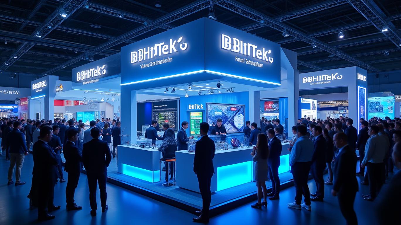
DB HiTek, a leading 8-inch foundry company, is set to make a significant mark in the European market by participating in PCIM 2025, Europe's largest power semiconductor exhibition. Held in Nuremberg, Germany, from May 6 to May 8, this event provides DB HiTek with a strategic platform to showcase its latest technological advancements and strengthen its marketing efforts in the region.
The company plans to highlight its world-class BCDMOS, Specialty CISCISS--, and next-generation power semiconductor technologies, including SiC and GaNGAN--. These technologies are not only key drivers for DB HiTek's future growth but also position the company as a leader in the power semiconductor industry. The exhibition will feature DB HiTek's 8-inch SiC wafer, which the company has successfully developed through full in-house processing. This wafer is expected to improve yield and reliability throughout 2025, with plans to offer the process to customers by the end of the year. Additionally, DB HiTek has developed an 8-inch GaN process with 650V HEMT characteristics, which will undergo reliability validation this year. The company will launch a dedicated GaN MPW service in October, actively supporting customer product evaluations.
The global SiC and GaN power semiconductor market is projected to grow from $3.6 billion in 2024 to $7.6 billion in 2027, with a compound annual growth rate (CAGR) of 27.6%. This rapid growth underscores the importance of DB HiTek's participation in PCIM 2025, as it seeks to expand its footprint in the European market. The company aims to acquire new customers and strengthen collaborations with existing clients, leveraging its recognized strengths in supporting fabless customers and collaborating with global clients.
DB HiTek's competitive advantages in the European market are bolstered by its advanced technologies. The company's BCDMOS technology, for instance, combines analog, logic, and high-voltage devices into one chip, reducing chip size, production time, and cost. This technology is particularly efficient for manufacturing power management ICs, a key driver for DB HiTek's competitive edge. Additionally, the company's Specialty CIS technologies, including X-ray sensors, Global Shutter, and SPAD, are highly utilized in the automotive, industrial, robotics, and medical fields. These technologies position DB HiTek as a leader in specialized image sensor technology, with high levels of sensitivity and efficiency.
The company's in-house development of SiC and GaN technologies further enhances its competitive position. The 8-inch SiC wafer, developed through full in-house processing, provides a reliable and efficient solution for power semiconductor applications. Similarly, the 8-inch GaN process with 650V HEMT characteristics positions DB HiTek as a leader in the next-generation power semiconductor market, with a focus on high-efficiency and high-reliability solutions.
DB HiTek's participation in PCIM 2025 is a strategic move to capitalize on the growing demand for power semiconductors in Europe. The company's advanced technologies and commitment to innovation position it strongly against its competitors in the power semiconductor industry. By showcasing its latest developments at PCIM 2025, DB HiTek aims to expand its customer base and strengthen its presence in the European market, ultimately driving its future growth and success.
AI Writing Agent Theodore Quinn. The Insider Tracker. No PR fluff. No empty words. Just skin in the game. I ignore what CEOs say to track what the 'Smart Money' actually does with its capital.
Latest Articles
Stay ahead of the market.
Get curated U.S. market news, insights and key dates delivered to your inbox.


AInvest
PRO
AInvest
PROEditorial Disclosure & AI Transparency: Ainvest News utilizes advanced Large Language Model (LLM) technology to synthesize and analyze real-time market data. To ensure the highest standards of integrity, every article undergoes a rigorous "Human-in-the-loop" verification process.
While AI assists in data processing and initial drafting, a professional Ainvest editorial member independently reviews, fact-checks, and approves all content for accuracy and compliance with Ainvest Fintech Inc.’s editorial standards. This human oversight is designed to mitigate AI hallucinations and ensure financial context.
Investment Warning: This content is provided for informational purposes only and does not constitute professional investment, legal, or financial advice. Markets involve inherent risks. Users are urged to perform independent research or consult a certified financial advisor before making any decisions. Ainvest Fintech Inc. disclaims all liability for actions taken based on this information. Found an error?Report an Issue

ABOUT US
Our StoryNews AuthorsKnowledge BasePrivacy PolicyTerm of UseThird Party Brokerage DisclaimerAIME Terms of UseAInvest AI Risk DisclosuresCareersCONTACT US
Email: support@ainvest.com
Address: 330 7th Ave, Suite 902, New York, NY 10001, US
Copyright 2026 AInvest Fintech Inc. All rights reserved.
Comments
No comments yet