
STMicroelectronics: Pioneering the Future of Silicon Photonics in Europe's 300mm Wafer Revolution
In an era where data is the lifeblood of global economies, the race to develop next-generation infrastructure for high-speed, low-power data transmission has intensified. At the forefront of this revolution is STMicroelectronics, a European semiconductor leader leveraging its strategic position in the STARLight Project to cement its dominance in the high-growth 300mm silicon photonics (SiPho) market. With the European Union's CHIPS Act providing a $1B funding umbrella, ST is not only advancing its technological edge but also reshaping the competitive landscape for global semiconductor players.
The STARLight Project: A Strategic Power Play
The STARLight Project, led by STMicroelectronicsSTM-- and involving 24 partners from 11 EU countries, represents a $1B bet on Europe's semiconductor sovereignty. According to a report by STMicroelectronics, the consortium aims to establish a high-volume manufacturing line for 300mm silicon photonics by 2028, targeting applications in datacenters, AI clusters, telecommunications, and automotive markets [1]. This initiative is critical for addressing the growing demand for 200 Gbps+ modulators, on-chip lasers, and advanced photonic integrated circuits (PICs) [2].
ST's leadership in STARLight is underpinned by its expertise in Silicon-on-Insulator (SOI) and its exploration of Lithium Niobate (LNOI) and Barium Titanate (BTO) materials, which promise to overcome traditional silicon substrate limitations [3]. By collaborating with industry giants like NVIDIA, Ericsson, and CEA-LETI, ST is aligning its R&D with real-world application needs, ensuring its solutions are both cutting-edge and commercially viable [4].
Market Dynamics: A $10B Opportunity by 2030
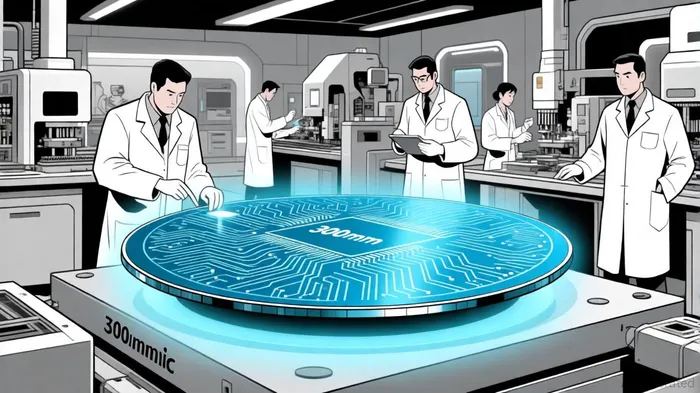
The global silicon photonics market is projected to grow at a CAGR of 25.8–29.5% from 2025 to 2030, reaching $8.13–$10.36 billion by 2030, driven by AI datacenters, 5G networks, and energy-efficient interconnects [5]. STMicroelectronics is uniquely positioned to capitalize on this growth. Its IDM (Integrated Device Manufacturer) model allows it to control both design and manufacturing, ensuring rapid iteration and cost efficiency. For instance, ST's PIC100 and B55(X) platforms, produced at its 300mm fab in Crolles, France, are already enabling 800Gb/s+ optical interconnects for cloud providers [6].
The company's expansion of 300mm wafer production—doubling capacity to 4,000 wafers/week by 2027 in Agrate, Italy, and scaling to 20,000 wafers/week by 2030 in Crolles—aligns with industry forecasts predicting a $13.23 billion 300mm wafer market by 2033 [7]. This vertical integration reduces dependency on third-party foundries and positions ST to meet surging demand for silicon photonics in AI and automotive sectors.
Competitive Advantages: Beyond the Chip
While competitors like Intel and Broadcom dominate the silicon photonics space, ST's STARLight-led consortium offers a unique edge. Unlike Intel's focus on high-volume transceivers or Broadcom's acquisition-driven strategy, ST is building a European ecosystem for silicon photonics, supported by EU funding and strategic partnerships. This reduces geopolitical risks and accelerates time-to-market for EU-based clients.
Moreover, ST's foundry model—providing key building blocks (e.g., PICs) rather than end products—positions it as a critical enabler for cloud providers and telecom firms. As noted in a Grand View Research analysis, the demand for energy-efficient, high-bandwidth solutions is pushing companies to adopt silicon photonics over traditional copper interconnects [8]. ST's ability to integrate on-chip lasers and modulators into a single platform further enhances its value proposition.
Risks and Mitigations
Despite its strengths, ST faces challenges. High R&D costs and integration complexities in silicon photonics could delay timelines. However, the EU CHIPS Act's $1B funding and ST's AI-driven manufacturing optimization mitigate these risks [9]. Additionally, the company's focus on modular fab expansions allows it to scale production incrementally, aligning with market demand.
Conclusion: A Long-Term Investment Thesis
STMicroelectronics' leadership in the STARLight Project and its strategic investments in 300mm silicon photonics position it as a must-watch player in the semiconductor industry. With the EU's backing, a $10B+ market opportunity, and a vertically integrated model, ST is poised to capture significant revenue growth while reinforcing Europe's technological sovereignty. For investors, this represents a compelling long-term bet on the infrastructure underpinning the AI and data-driven future.


Comentarios
Aún no hay comentarios