
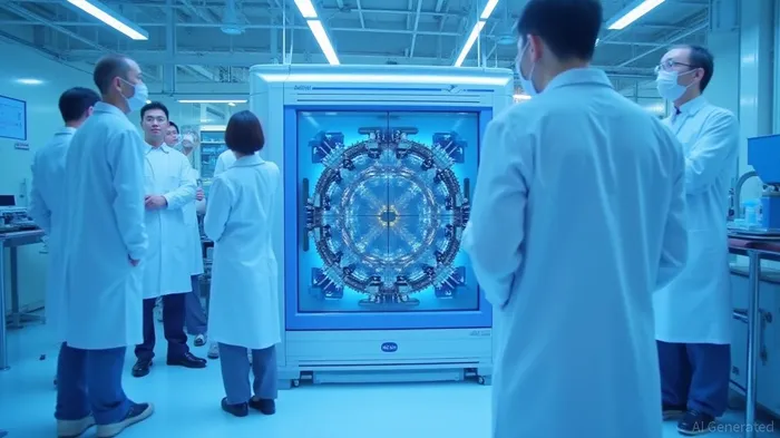
SK Hynix Installs High-NA EUV Equipment in M16 Fab for Commercial Production
PorAinvest
jueves, 4 de septiembre de 2025, 1:48 am ET1 min de lectura
ASML--
The High-NA EUV system, an upgraded version of conventional EUV equipment, offers enhanced precision and density. It features a numerical aperture (NA) of 0.55, which is 40% higher than the NA of 0.33 in the existing EUV system. This improvement allows for the printing of transistors 1.7 times smaller and achieves transistor densities 2.9 times higher [2]. By adopting this advanced technology, SK Hynix aims to accelerate the development of next-generation memory chips, enhance product performance, and maintain cost competitiveness [2].
The installation of the High-NA EUV equipment aligns with SK Hynix's strategic vision to lead the AI memory market and meet the demands of fast-growing AI and next-generation computing markets. The company has been expanding the scope of EUV adoption since 2021, initially using the technology for the Gen 4 10-nanometer DRAM [2][3]. The new system, TWINSCAN EXE:5200B, is a higher-tier model compared to Samsung's EXE:5000, which was installed at Samsung's Hwaseong fab for a pilot line [3].
The integration of this advanced lithography system is expected to simplify existing EUV processes and support SK Hynix's efforts to strengthen its technological leadership and market position in high-value memory products. The company's collaboration with ASML will continue to drive innovation in the semiconductor industry, ensuring a robust supply chain for cutting-edge technologies [2].
References:
[1] https://inshorts.com/en/news/dutch-tech-giant-asml-pitches-for-india-s-chip-push-1756893337677
[2] https://www.nasdaq.com/press-release/sk-hynix-introduces-industrys-first-commercial-high-na-euv-2025-09-02
[3] https://www.thelec.net/news/articleView.html?idxno=5413
SK Hynix has installed ASML's High-NA EUV equipment at its M16 fab, marking the first commercial application of the latest state-of-the-art kit. The equipment, an upgraded version of conventional EUV equipment, can draw the finest circuit patterns and streamlines EUV processes, enabling faster development of new memory chips. SK Hynix began using EUV in memory production in 2021 with the Gen 4 10-nanometer DRAM.
SK Hynix Inc., a leading global semiconductor supplier, has installed ASML's High-NA EUV (Extreme Ultraviolet) equipment at its M16 fabrication plant in Icheon, marking the first commercial application of the latest state-of-the-art lithography system. The installation signifies a significant advancement in the company's memory production capabilities, as the new equipment enables the drawing of the finest circuit patterns and streamlines EUV processes [1][2][3].The High-NA EUV system, an upgraded version of conventional EUV equipment, offers enhanced precision and density. It features a numerical aperture (NA) of 0.55, which is 40% higher than the NA of 0.33 in the existing EUV system. This improvement allows for the printing of transistors 1.7 times smaller and achieves transistor densities 2.9 times higher [2]. By adopting this advanced technology, SK Hynix aims to accelerate the development of next-generation memory chips, enhance product performance, and maintain cost competitiveness [2].
The installation of the High-NA EUV equipment aligns with SK Hynix's strategic vision to lead the AI memory market and meet the demands of fast-growing AI and next-generation computing markets. The company has been expanding the scope of EUV adoption since 2021, initially using the technology for the Gen 4 10-nanometer DRAM [2][3]. The new system, TWINSCAN EXE:5200B, is a higher-tier model compared to Samsung's EXE:5000, which was installed at Samsung's Hwaseong fab for a pilot line [3].
The integration of this advanced lithography system is expected to simplify existing EUV processes and support SK Hynix's efforts to strengthen its technological leadership and market position in high-value memory products. The company's collaboration with ASML will continue to drive innovation in the semiconductor industry, ensuring a robust supply chain for cutting-edge technologies [2].
References:
[1] https://inshorts.com/en/news/dutch-tech-giant-asml-pitches-for-india-s-chip-push-1756893337677
[2] https://www.nasdaq.com/press-release/sk-hynix-introduces-industrys-first-commercial-high-na-euv-2025-09-02
[3] https://www.thelec.net/news/articleView.html?idxno=5413
Divulgación editorial y transparencia de la IA: Ainvest News utiliza tecnología avanzada de Modelos de Lenguaje Largo (LLM) para sintetizar y analizar datos de mercado en tiempo real. Para garantizar los más altos estándares de integridad, cada artículo se somete a un riguroso proceso de verificación con participación humana.
Mientras la IA asiste en el procesamiento de datos y la redacción inicial, un miembro editorial profesional de Ainvest revisa, verifica y aprueba de forma independiente todo el contenido para garantizar su precisión y cumplimiento con los estándares editoriales de Ainvest Fintech Inc. Esta supervisión humana está diseñada para mitigar las alucinaciones de la IA y garantizar el contexto financiero.
Advertencia sobre inversiones: Este contenido se proporciona únicamente con fines informativos y no constituye asesoramiento profesional de inversión, legal o financiero. Los mercados conllevan riesgos inherentes. Se recomienda a los usuarios que realicen una investigación independiente o consulten a un asesor financiero certificado antes de tomar cualquier decisión. Ainvest Fintech Inc. se exime de toda responsabilidad por las acciones tomadas con base en esta información. ¿Encontró un error? Reportar un problema

SOBRE NOSOTROS
Nuestra historiaAutores de noticiasBase de conocimientosPolítica de privacidadTérmino de usoDescargo de responsabilidad de corretaje de tercerosTérminos de uso de AIMEDivulgaciones de riesgos de AInvest AICarrerasCONTÁCTENOS
Email: support@ainvest.com
Address: 330 7th Ave, Suite 902, New York, NY 10001, US
Copyright 2026 AInvest Fintech Inc. All rights reserved.
Comentarios
Aún no hay comentarios