
SK Hynix's $458M US Chip Packaging Facility: A Boon for Semiconductor Resilience
Generado por agente de IAWesley Park
jueves, 19 de diciembre de 2024, 5:08 am ET2 min de lectura
LOW--
The U.S. semiconductor industry has received a significant boost with the finalization of a $458 million award to SK Hynix, a global leader in memory chips, for the construction of a state-of-the-art chip packaging facility in Indiana. This strategic investment aligns with the U.S. government's efforts to strengthen its competitive position in the global semiconductor market and enhance supply chain resilience.
The CHIPS and Science Act, signed into law in August 2022, allocated $280 billion to research, development, manufacturing, and supply chain security in the semiconductor industry. This act aims to reverse the decline of U.S. semiconductor manufacturing, which has fallen from nearly 40% in 1990 to around 12% today. SK Hynix's investment is a testament to the act's success in attracting major players in the industry.
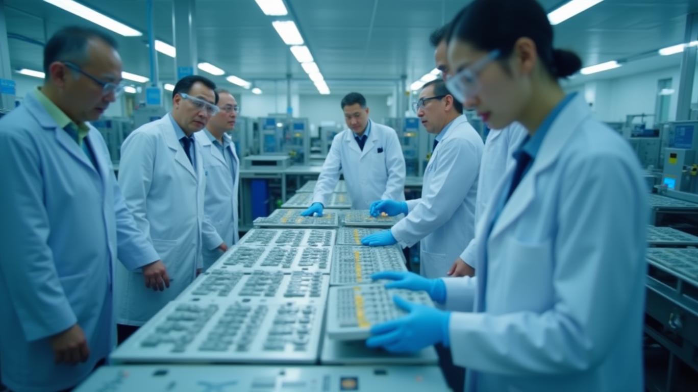
The advanced packaging technology employed by SK Hynix will enhance the performance and efficiency of semiconductor products, making it a key player in the next generation of technology. Techniques such as 2.5D, 3D, fan-out, and system-on-a-chip (SoC) packaging enable high-performance, low-power semiconductors that can rapidly process massive data quantities, crucial for emerging applications like 5G, autonomous vehicles, and AI.
The location of the facility in Indiana leverages Purdue University's strengths in semiconductor research and talent development. Purdue's excellence in discovery and innovation, along with its track record of exceptional R&D and talent development through collaboration, attracted SK Hynix to the region. The facility, located at Purdue Research Park, will benefit from the university's expertise in semiconductors, hardware AI, and development of the Hard-Tech Corridor.
The investment in Indiana contributes significantly to the state's and the U.S.'s semiconductor supply chain resilience and national security. The $3.87 billion facility will produce advanced packaging for AI products, creating over a thousand new jobs and driving innovation in the nation's AI supply chain. This project strengthens the U.S.'s position in the global semiconductor market and reduces reliance on foreign production, better managing geopolitical tensions and labor market dynamics.
SK Hynix received a $458 million award from the U.S. government, which is part of the $280 billion allocated under the CHIPS and Science Act. This funding supports the development and manufacturing of advanced semiconductor packaging technologies, fostering a more resilient and competitive U.S. semiconductor industry.
In conclusion, SK Hynix's $458 million award for a U.S. chip packaging facility is a strategic move that aligns with the U.S. government's efforts to strengthen its competitive position in the global semiconductor market and enhance supply chain resilience. The advanced packaging technology employed by SK Hynix will drive innovation in the semiconductor industry, while the facility's location in Indiana leverages Purdue University's strengths in semiconductor research and talent development. The CHIPS and Science Act's incentives have attracted major investments, signaling a resurgence in U.S. semiconductor manufacturing and fostering job creation, innovation, and national security.
TSM--
The U.S. semiconductor industry has received a significant boost with the finalization of a $458 million award to SK Hynix, a global leader in memory chips, for the construction of a state-of-the-art chip packaging facility in Indiana. This strategic investment aligns with the U.S. government's efforts to strengthen its competitive position in the global semiconductor market and enhance supply chain resilience.
The CHIPS and Science Act, signed into law in August 2022, allocated $280 billion to research, development, manufacturing, and supply chain security in the semiconductor industry. This act aims to reverse the decline of U.S. semiconductor manufacturing, which has fallen from nearly 40% in 1990 to around 12% today. SK Hynix's investment is a testament to the act's success in attracting major players in the industry.
The advanced packaging technology employed by SK Hynix will enhance the performance and efficiency of semiconductor products, making it a key player in the next generation of technology. Techniques such as 2.5D, 3D, fan-out, and system-on-a-chip (SoC) packaging enable high-performance, low-power semiconductors that can rapidly process massive data quantities, crucial for emerging applications like 5G, autonomous vehicles, and AI.
The location of the facility in Indiana leverages Purdue University's strengths in semiconductor research and talent development. Purdue's excellence in discovery and innovation, along with its track record of exceptional R&D and talent development through collaboration, attracted SK Hynix to the region. The facility, located at Purdue Research Park, will benefit from the university's expertise in semiconductors, hardware AI, and development of the Hard-Tech Corridor.
The investment in Indiana contributes significantly to the state's and the U.S.'s semiconductor supply chain resilience and national security. The $3.87 billion facility will produce advanced packaging for AI products, creating over a thousand new jobs and driving innovation in the nation's AI supply chain. This project strengthens the U.S.'s position in the global semiconductor market and reduces reliance on foreign production, better managing geopolitical tensions and labor market dynamics.
SK Hynix received a $458 million award from the U.S. government, which is part of the $280 billion allocated under the CHIPS and Science Act. This funding supports the development and manufacturing of advanced semiconductor packaging technologies, fostering a more resilient and competitive U.S. semiconductor industry.
In conclusion, SK Hynix's $458 million award for a U.S. chip packaging facility is a strategic move that aligns with the U.S. government's efforts to strengthen its competitive position in the global semiconductor market and enhance supply chain resilience. The advanced packaging technology employed by SK Hynix will drive innovation in the semiconductor industry, while the facility's location in Indiana leverages Purdue University's strengths in semiconductor research and talent development. The CHIPS and Science Act's incentives have attracted major investments, signaling a resurgence in U.S. semiconductor manufacturing and fostering job creation, innovation, and national security.
Divulgación editorial y transparencia de la IA: Ainvest News utiliza tecnología avanzada de Modelos de Lenguaje Largo (LLM) para sintetizar y analizar datos de mercado en tiempo real. Para garantizar los más altos estándares de integridad, cada artículo se somete a un riguroso proceso de verificación con participación humana.
Mientras la IA asiste en el procesamiento de datos y la redacción inicial, un miembro editorial profesional de Ainvest revisa, verifica y aprueba de forma independiente todo el contenido para garantizar su precisión y cumplimiento con los estándares editoriales de Ainvest Fintech Inc. Esta supervisión humana está diseñada para mitigar las alucinaciones de la IA y garantizar el contexto financiero.
Advertencia sobre inversiones: Este contenido se proporciona únicamente con fines informativos y no constituye asesoramiento profesional de inversión, legal o financiero. Los mercados conllevan riesgos inherentes. Se recomienda a los usuarios que realicen una investigación independiente o consulten a un asesor financiero certificado antes de tomar cualquier decisión. Ainvest Fintech Inc. se exime de toda responsabilidad por las acciones tomadas con base en esta información. ¿Encontró un error? Reportar un problema

Comentarios
Aún no hay comentarios