
SK Hynix's $13B Bet: Securing a Critical AI Infrastructure Layer
The investment thesis here is about securing a fundamental rail for the next technological paradigm. SK Hynix's $13 billion packaging plant is a necessary, first-mover bet to ensure its role as a critical infrastructure layer in the AI supercycle. This isn't just about building a factory; it's about capturing the exponential adoption curve of AI memory itself.
The demand curve is defined by a staggering growth rate. The high-bandwidth memory (HBM) market, the specialized memory that powers AI accelerators, is projected to expand at a compound annual growth rate of 33% from 2025 to 2030. That's a classic S-curve inflection point, where adoption accelerates from niche to essential. SK Hynix is positioning itself directly on that steep part of the curve.
Its strategic importance is cemented by its role as a key supplier to NvidiaNVDA--, the primary driver of this memory supercycle. The company is among the world's largest producers of memory chips and leads in so-called high-bandwidth memory (HBM), which is used in Nvidia's AI processors. By building this capacity now, SK Hynix is locking in its position as a foundational supplier before the next wave of AI compute demands outstrips supply.
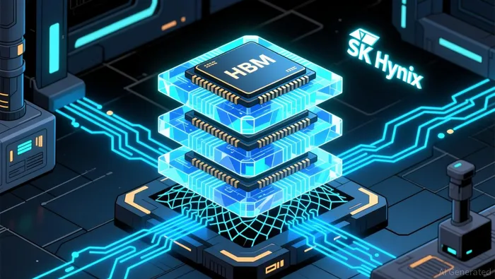
The new P&T7 facility in Cheongju is the physical manifestation of this strategy. This advanced packaging fab is essential for the final stages of manufacturing AI memory products. It will complete semiconductor chips produced in a full-process fab into final product form, integrating multiple memory chips into a single, high-density unit. With construction set to begin in April and completion targeted for the end of 2027, the plant is a multi-year commitment to meet the surging demand that has already pushed prices up and created a lucrative cycle for memory giants. This is infrastructure built for exponential growth.
The Packaging Bottleneck: A New Frontier in Semiconductor Value
The semiconductor industry is undergoing a fundamental shift in where value is created. The focus is moving decisively from pure fabrication to advanced packaging, where the final integration of complex chips into functional units is becoming the critical bottleneck. This transition is being driven by the insatiable demand of AI, which requires packaging technologies like CoWoS to stack multiple memory dies into high-density, high-performance units. The market for the equipment that enables this packaging is expanding rapidly, with sales forecast to grow by more than 10% in 2024 and potentially exceed 20% in 2025.
The scale of this demand is staggering. Global demand for CoWoS packaging wafers alone is projected to reach 1 million units by 2026. The lion's share of this capacity is already spoken for, with Nvidia securing a commanding 595,000 wafers-about 60% of the total. This isn't just a supply contract; it's a strategic lock-in for the foundational memory needed to power its next-generation AI chips. The competition for this infrastructure layer is fierce, with other major players like Broadcom and AMD also securing significant allocations.
Against this backdrop, SK Hynix's $13 billion investment in its P&T7 packaging plant is a direct response to this new value frontier. The company is not just building a factory; it is building a critical node in the AI memory supply chain. This move comes as its key rival, Samsung, is also aggressively expanding. Samsung plans to ramp up its HBM production capacity by 50% in 2026, aiming to produce around 250,000 wafers per month by year-end. This parallel expansion by both giants underscores that advanced packaging and HBM production are now the primary battleground for securing a role in the AI paradigm shift.
The bottom line is that the semiconductor value chain has bifurcated. While front-end fabrication remains capital-intensive, the bottleneck-and the next wave of profit-lies in the packaging stage. SK Hynix's massive bet is a calculated play to capture a disproportionate share of that value as the AI supercycle accelerates.
Financial and Competitive Impact: Scaling for the Super-Cycle
The financial commitment is massive, but the market is pricing in the payoff. SK Hynix's $13 billion investment-equivalent to 19 trillion won-is a direct capital allocation to meet the surging demand that defines this multi-year memory supercycle. The company is not just building a factory; it is building the physical infrastructure to capture exponential growth. This move is backed by a clear financial trajectory, with HSBC analyst Ricky Seo projecting a record fourth-quarter operating profit of 18 trillion won, up 57% from the prior quarter. The stock's performance reflects this optimism, with shares up around 13% so far this year. Yet the recent pullback-down 1.6% on Tuesday amid profit-taking-shows the market is already pricing in this success, leaving little room for disappointment.
Competitively, the stakes are high. The company is racing against a rival that is also doubling down. Samsung has announced plans to ramp up its HBM production capacity by 50% in 2026, aiming for a massive output. This parallel expansion by both giants underscores that the battle for AI memory dominance is now a two-horse race for the critical packaging and final integration layer. SK Hynix's $13 billion bet is a necessary counter-move to maintain its lead as a key supplier to Nvidia and secure its position on the steep part of the HBM adoption curve.
Looking beyond its current capital base, the company is also considering a strategic move to access even deeper pools of global capital. SK Hynix is weighing a potential U.S. listing following a blockbuster 2025 for its shares. This would be a classic infrastructure play, allowing the company to fund its massive, multi-year build-out with the liquidity of a global market. It signals a forward-looking ambition to finance the next phase of the AI supercycle from the very start.
Catalysts, Risks, and What to Watch
The investment thesis now hinges on a multi-year execution timeline. The primary catalyst is the successful ramp of the P&T7 facility by the end of 2027. This plant is not just a capacity adder; it is a direct response to the next wave of AI compute. Its completion will coincide with the adoption of HBM4, the next-generation memory standard, and the launch of Nvidia's Rubin chip. By having its advanced packaging capacity ready, SK Hynix can capture the initial surge of demand for these new products, locking in long-term supply contracts and maintaining its critical infrastructure role.
The most significant risk is execution on a $13 billion project with a 2027 completion date. Any delay in construction or qualification would be costly, as the HBM market is moving fast. Samsung is already planning a 50% ramp in its HBM production capacity in 2026, aiming for a massive output. A delay from SK Hynix could cede valuable market share to its rival or even to TSMC, which is also a key player in advanced packaging. The company's own history of production challenges, noted in the evidence, underscores that scaling complex processes is never guaranteed.
The key watchpoint for investors is quarterly HBM shipments and average selling price (ASP) trends. These metrics will directly gauge whether the projected 33% annual market growth is materializing. Consistent shipment growth above the forecasted rate would validate the super-cycle thesis and the timing of the P&T7 investment. Conversely, any deviation-especially a slowdown in ASPs due to competitive pressure or a shift in product mix-would signal that the exponential adoption curve is steeper than expected, potentially forcing a reassessment of the build-out's pace and profitability. The next few quarters will be critical for confirming the trajectory.

Comentarios
Aún no hay comentarios