
DB HiTek: Expanding European Footprint at PCIM 2025
Generado por agente de IATheodore Quinn
domingo, 6 de abril de 2025, 9:15 pm ET2 min de lectura
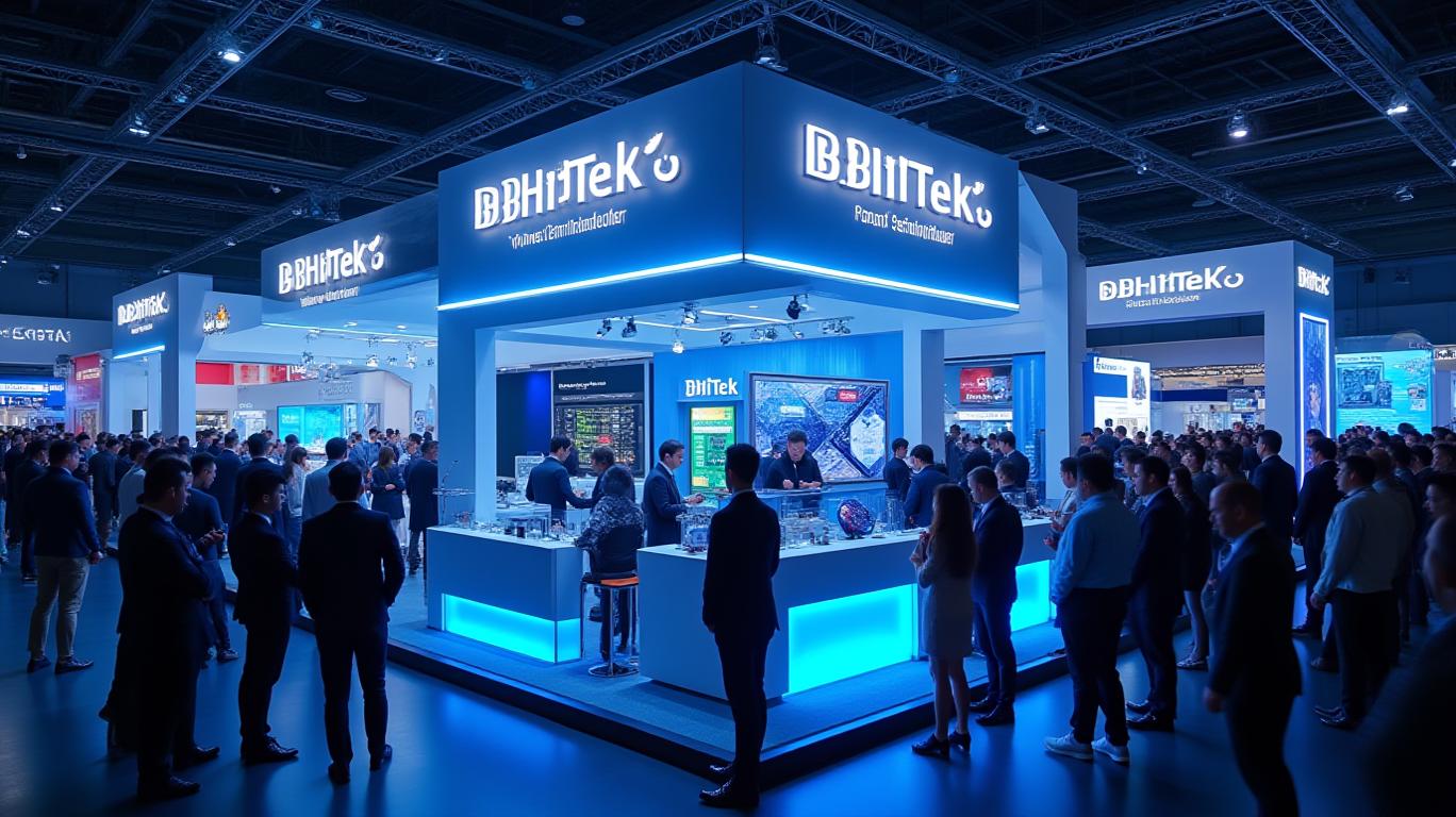
DB HiTek, a leading 8-inch foundry company, is set to make a significant mark in the European market by participating in PCIM 2025, Europe's largest power semiconductor exhibition. Held in Nuremberg, Germany, from May 6 to May 8, this event provides DB HiTek with a strategic platform to showcase its latest technological advancements and strengthen its marketing efforts in the region.
The company plans to highlight its world-class BCDMOS, Specialty CISCISS--, and next-generation power semiconductor technologies, including SiC and GaNGAN--. These technologies are not only key drivers for DB HiTek's future growth but also position the company as a leader in the power semiconductor industry. The exhibition will feature DB HiTek's 8-inch SiC wafer, which the company has successfully developed through full in-house processing. This wafer is expected to improve yield and reliability throughout 2025, with plans to offer the process to customers by the end of the year. Additionally, DB HiTek has developed an 8-inch GaN process with 650V HEMT characteristics, which will undergo reliability validation this year. The company will launch a dedicated GaN MPW service in October, actively supporting customer product evaluations.
The global SiC and GaN power semiconductor market is projected to grow from $3.6 billion in 2024 to $7.6 billion in 2027, with a compound annual growth rate (CAGR) of 27.6%. This rapid growth underscores the importance of DB HiTek's participation in PCIM 2025, as it seeks to expand its footprint in the European market. The company aims to acquire new customers and strengthen collaborations with existing clients, leveraging its recognized strengths in supporting fabless customers and collaborating with global clients.
DB HiTek's competitive advantages in the European market are bolstered by its advanced technologies. The company's BCDMOS technology, for instance, combines analog, logic, and high-voltage devices into one chip, reducing chip size, production time, and cost. This technology is particularly efficient for manufacturing power management ICs, a key driver for DB HiTek's competitive edge. Additionally, the company's Specialty CIS technologies, including X-ray sensors, Global Shutter, and SPAD, are highly utilized in the automotive, industrial, robotics, and medical fields. These technologies position DB HiTek as a leader in specialized image sensor technology, with high levels of sensitivity and efficiency.
The company's in-house development of SiC and GaN technologies further enhances its competitive position. The 8-inch SiC wafer, developed through full in-house processing, provides a reliable and efficient solution for power semiconductor applications. Similarly, the 8-inch GaN process with 650V HEMT characteristics positions DB HiTek as a leader in the next-generation power semiconductor market, with a focus on high-efficiency and high-reliability solutions.
DB HiTek's participation in PCIM 2025 is a strategic move to capitalize on the growing demand for power semiconductors in Europe. The company's advanced technologies and commitment to innovation position it strongly against its competitors in the power semiconductor industry. By showcasing its latest developments at PCIM 2025, DB HiTek aims to expand its customer base and strengthen its presence in the European market, ultimately driving its future growth and success.


Divulgación editorial y transparencia de la IA: Ainvest News utiliza tecnología avanzada de Modelos de Lenguaje Largo (LLM) para sintetizar y analizar datos de mercado en tiempo real. Para garantizar los más altos estándares de integridad, cada artículo se somete a un riguroso proceso de verificación con participación humana.
Mientras la IA asiste en el procesamiento de datos y la redacción inicial, un miembro editorial profesional de Ainvest revisa, verifica y aprueba de forma independiente todo el contenido para garantizar su precisión y cumplimiento con los estándares editoriales de Ainvest Fintech Inc. Esta supervisión humana está diseñada para mitigar las alucinaciones de la IA y garantizar el contexto financiero.
Advertencia sobre inversiones: Este contenido se proporciona únicamente con fines informativos y no constituye asesoramiento profesional de inversión, legal o financiero. Los mercados conllevan riesgos inherentes. Se recomienda a los usuarios que realicen una investigación independiente o consulten a un asesor financiero certificado antes de tomar cualquier decisión. Ainvest Fintech Inc. se exime de toda responsabilidad por las acciones tomadas con base en esta información. ¿Encontró un error? Reportar un problema

SOBRE NOSOTROS
Nuestra historiaAutores de noticiasBase de conocimientosPolítica de privacidadTérmino de usoDescargo de responsabilidad de corretaje de tercerosTérminos de uso de AIMEDivulgaciones de riesgos de AInvest AICarrerasCONTÁCTENOS
Email: support@ainvest.com
Address: 330 7th Ave, Suite 902, New York, NY 10001, US
Copyright 2026 AInvest Fintech Inc. All rights reserved.
Comentarios
Aún no hay comentarios