
Applied Materials and GlobalFoundries: Pioneering the Photonics Revolution in Semiconductor Manufacturing
The semiconductor industry is on the cusp of a transformative era, driven by the convergence of artificial intelligence (AI), augmented reality (AR), and photonics. At the forefront of this shift is the strategic collaboration between Applied Materials and GlobalFoundries in Singapore, a partnership that signals a pivotal investment in next-generation chip fabrication and the broader photonics ecosystem. By combining Applied Materials' expertise in materials science with GlobalFoundries' global manufacturing capabilities, the two firms are positioning themselves to capitalize on the exponential growth of silicon photonics—a technology poised to redefine data transmission, energy efficiency, and AI hardware innovation.
The Strategic Imperative: Photonics as the New Frontier
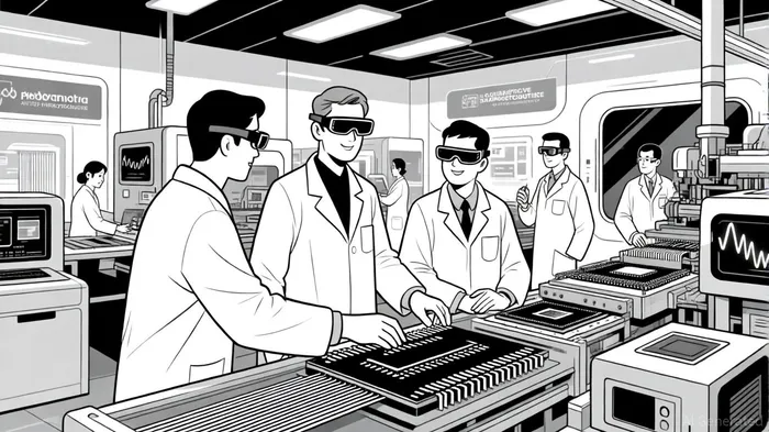
Photonics, the science of manipulating light for data transmission and processing, is emerging as a critical enabler for AI and AR applications. Traditional electronic interconnects are increasingly inadequate for the bandwidth demands of AI data centers and AR devices, which require ultra-low latency and high-speed communication. Applied MaterialsAMAT-- and GlobalFoundries' joint venture in Singapore aims to address this gap by establishing a state-of-the-art waveguide fabrication facility. This facility will focus on developing photonic components such as optical sensors, waveguides, and integrated circuits tailored for AI-powered AR glasses and high-performance computing systems [1].
Dr. Paul Meissner of Applied Materials has emphasized that photonics is "a cornerstone for human-centric AI experiences," particularly in AR devices where real-time data processing and immersive user interfaces are paramount [3]. Meanwhile, GlobalFoundries' Yew Kong Tan highlighted the partnership's potential to "deliver scalable solutions for next-generation devices," underscoring the strategic alignment between materials innovation and manufacturing execution [2].
Market Dynamics: A $54 Billion Opportunity by 2035
The financial implications of this collaboration are underscored by the explosive growth of the photonic integrated circuit (PIC) market. According to a report by Laser Focus World, the PIC market is projected to surpass $54 billion by 2035, driven by AI data centers' insatiable demand for high-bandwidth, low-latency communication channels [2]. Silicon photonics, in particular, is gaining traction due to its compatibility with existing semiconductor fabrication processes, enabling cost-effective scaling.
The global silicon photonics market, valued at $1.29 billion in 2022, is expected to grow at a compound annual rate of 25.8%, reaching $8.13 billion by 2030 [2]. This growth is fueled by the need for energy-efficient solutions in data centers, where AI models and accelerators generate massive data flows. For instance, co-packaged optics (CPO)—a technology that integrates photonics with electronic components—has emerged as a key innovation, reducing signal loss and power consumption in AI infrastructure [2].
Strategic Partnerships and the Foundry Ecosystem
The Applied Materials-GlobalFoundries collaboration exemplifies a broader trend in semiconductor manufacturing: the rise of ecosystem-driven partnerships. As AI accelerators are projected to account for nearly 50% of data center semiconductor revenue by 2030 [3], companies are prioritizing vertical integration and cross-industry alliances to secure supply chains and accelerate R&D.
Singapore's selection as the site for this venture is no coincidence. The city-state has emerged as a global hub for photonics innovation, with government-backed initiatives fostering collaboration between academia, startups, and multinational corporations. By anchoring their partnership in Singapore, Applied Materials and GlobalFoundriesGFS-- are not only leveraging local expertise but also aligning with regional efforts to build a self-sustaining photonics ecosystem that spans materials, sensors, and end-user applications [4].
Investment Implications: Advanced Materials as a Catalyst
For investors, the partnership highlights the growing importance of advanced materials in semiconductor innovation. Applied Materials' leadership in materials engineering—ranging from photonic waveguides to high-precision laser systems—positions it as a key enabler of next-generation fabrication processes. Meanwhile, GlobalFoundries' foundry capabilities ensure that these materials can be scaled efficiently, reducing the time-to-market for cutting-edge photonic components.
The semiconductor industry as a whole is witnessing a surge in capital expenditures, with global investments in fabrication facilities expected to exceed $1.5 trillion between 2024 and 2030 [3]. This trend is particularly pronounced in AI-driven sectors, where companies like Texas Instruments and Intel are doubling down on manufacturing capabilities. For Applied Materials and GlobalFoundries, the Singapore venture represents a strategic bet on a sector that is not only capital-intensive but also highly profitable, given the premium pricing of photonic and AI-optimized components.
Conclusion: A Blueprint for the Future
The Applied Materials-GlobalFoundries collaboration is more than a partnership—it is a blueprint for the future of semiconductor manufacturing. By focusing on photonics, the duo is addressing the fundamental limitations of traditional electronics while tapping into a market with multi-decade growth potential. For investors, this signals a compelling opportunity in advanced materials and foundry ecosystems, where innovation and scalability converge. As AI and AR reshape global technology landscapes, the companies that master photonics today will define the semiconductor industry of tomorrow.

Comentarios
Aún no hay comentarios