
Applied Materials' $2.0 Billion Credit Facility: Strategic Financing or Early Warning Signal?
In the semiconductor equipment manufacturing industry, where capital expenditures and R&D costs are as high as $1 billion per facility[1], financing decisions carry outsized implications. Applied Materials' recent $2.0 billion credit facility—replacing a $1.5 billion predecessor—has sparked debate: Is this a prudent move to secure growth in an AI-driven market, or a subtle signal of overreach in a sector already grappling with geopolitical and cyclical risks?
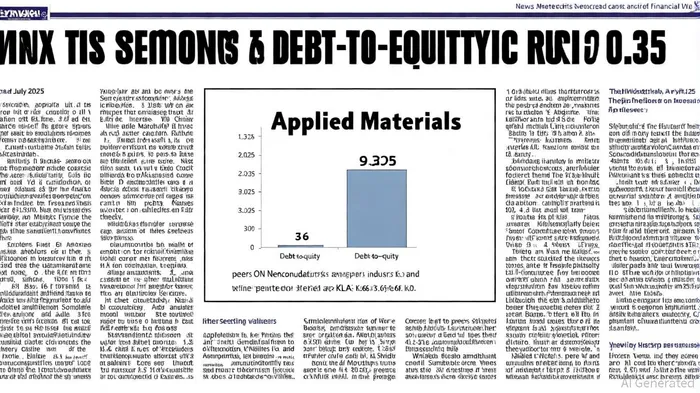
Capital Structure: Conservative Leverage, Robust Liquidity
Applied Materials' financial position appears resilient. As of July 2025, its debt-to-equity ratio stood at 0.35[2], slightly above the semiconductor equipment industry average of 0.3[3] but well below peers like KLA (3.06)[4]. This suggests a balanced approach to leverage, particularly when compared to companies like ON Semiconductor, which recently reported a 0.65 ratio[5].
Liquidity metrics reinforce this narrative. The company's current ratio of 2.68[6] and quick ratio of 1.62[7] as of late 2025 indicate ample short-term resources to cover obligations. These figures, combined with $9.054 billion in EBITDA for the twelve months ending July 2025[8], position Applied MaterialsAMAT-- to service debt comfortably. The new credit facility, which mandates maintaining an EBITDA-to-interest expense ratio of 3.00-to-1[9], aligns with these strengths.
Strategic Context: Credit Facilities in the Semiconductor Sector
The semiconductor industry's use of credit facilities often ties to strategic priorities. For instance, Intel and TSMC have leveraged CHIPS Act incentives—such as the 25% advanced manufacturing investment tax credit—to fund multi-billion-dollar fab expansions[10]. Similarly, Applied Materials' $2.0 billion facility could support R&D, M&A, or capital expenditures in a sector where R&D spending now accounts for 52% of EBIT[11].
However, the timing is telling. The company had previously announced a $4 billion R&D facility in Silicon Valley, only to reconsider it due to insufficient government funding[12]. The new credit facility may now serve as a contingency plan, offering flexibility to pursue projects without relying solely on public incentives. This aligns with broader industry trends: in 2024, semiconductor M&A surged to $45.4 billion in deal value[13], driven by AI infrastructure demands.
Risk Assessment: Sector Norms vs. Unique Pressures
While Applied Materials' leverage appears prudent, risks linger. The semiconductor equipment industry's average debt-to-equity ratio of 0.3[3] reflects a conservative profile, but companies like Sequans Communications SA (8.3 D/E)[14] demonstrate how aggressive financing can backfire. Applied Materials' facility, though modest relative to its $19.5 billion equity base[15], could become a concern if interest rates rise or demand for AI-driven semiconductors softens.
Moreover, the company's reliance on U.S. government incentives is a double-edged sword. While the CHIPS Act has spurred $540 billion in domestic investments[16], Applied Materials' R&D-focused projects may not qualify for the same level of support as manufacturing facilities[12]. This could force the company to depend more heavily on its credit line, potentially straining margins if ROI from R&D lags.
Conclusion: Strategic Prudence with Caution
Applied Materials' $2.0 billion credit facility is best viewed as a strategic hedge rather than a red flag. Its strong liquidity, conservative leverage, and alignment with industry trends—such as AI-driven R&D and M&A—suggest a calculated move to maintain competitiveness. However, investors should monitor how the facility is deployed. If used to fund high-risk ventures or if interest rate hikes pressure margins, the facility could shift from asset to liability. For now, though, the move appears to reflect the kind of proactive financial planning that defines leading semiconductor equipment firms in an era of rapid technological change.

Comentarios
Aún no hay comentarios